Low-energy ion implantation
 At the LMTS, we have pioneered the use of low energy filtered cathodic vacuum arc (FCVA) implantation to produce clean stretchable compliant electrodes that can easily be patterned on the micrometer scale via the use of shadow masks or through photolithography.
Based on an RHK ARC-20 FCVA source, our ion implanter sends gold ions at energies up to 10 keV into PDMS membranes, forming a gold-PDMS composite, which is conductive for ion doses above approximately 1015 ions/cm2, and can be stretched to almost three time its initial length while remaining a good conductor.
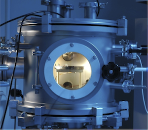
 In filtered cathodic vacuum arc implantation, a rod of the material that need to be implanted (the source) is inserted at the centre of a plasma gun. A high-voltage pulse is applied between a trigger ring and the source to create a plasma that triggers the main discharge between the anode and the source (cathode). The cathode is polarized at -600V through a bank of capacitors that discharges very quickly once the plasma is initiated. This high intensity current vaporizes the cathod material at its tip, thus creating a very dense plasma containing ions, electrons, and big and heavy macroparticles.
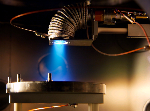
Our FCVA works in pulsed mode: once the capacitor bank has discharged the plasma quenches and the capacitor recharges. We typically implant with a pulse rate of 1-2 Hz.
Large macroparticles are unwanted on the substrate, and a filter is consequently used to trap them. It consists of a 90° bent tube with a coil wrapped around it. The coil is connected in series with the anode (one end to ground, the other to the anode). Each pulse (discharge of the capacitor bank) creates a high intensity current in the coil, this leading to a strong magnetic field along the coil. The electrons in the plasma are light enough to be affected by the magnetic field. The Lorentz force makes the electrons move in a coil-like path around the field line. The metal ion move with the electrons to which they are electrostatically attracted. The big macroparticles are too big (they have a very low charge over mass ratio) to be affected by the electron motion, and their trajectory is therefore unaffected: the collide with the filter walls. Only electrons and ions are able to escape the filter, thus ensuring purely ionic implantation.
 |
 |
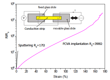
Implanted electrodes are compliant and conductive
The image below shows the resistivity of a narrow implanted line on PDMS as a function of strain, showing it conducts when its length is more than doubled (up to 175% strain). For comparison, the resistance of a sputtered gold line is also shown: the sputtered line breaks stops conducting at 4% strain due to cracks in the layer.
The conductivity and stiffness of implanted gold tracks are functions of the ion dose: high doses lead to lower electrical resistance, but to increased stiffness. The fascinating aspect of low-energy gold implantation is that thanks to the nanostructure obtained by this deposition technique, the stiffness of the membrane is about 5 times less than if an equivalent layer of gold had been evaporated on the surface of the same membrane.
The conductive electrodes thus made are ideal for micro-polymer actuators, because they allow the actuator to have large displacements (up to 100%), they can be patterned on the micron scale (using photolithography and lift-off), they are stable in time (not change in over 3 years), and can sustain many tens of thousands of repeated cycles.
metal-PDMS nanocomposite
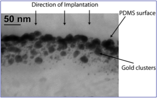
Transmission Electron Microscopy enables a detailed analysis of the gold-PDMS nanocomposite: how big are the particles? how deeply are they implanted? what fraction of gold is in the nanocomposite?
On the right, a TEM cross-section of an implanted PDMS membrane, showing the nanoparticles of gold resulting from a ion implantation, with dose 1.5 x10^16 ions/cm2, initial accelerating potential 2.5 keV per pulse.
The TEM cross-sections allow the microstructure to be quantified,which has enabled us to link measured macroscopic properties (resistivity, Young’s modulus) with the nanostructure.
TEM cross-sections were made for a wide range of doses and energies. Nanoparticles size with increases with ion dose, from an averag size of 5 nm up to 30 nm for nealry metallic films. See Niklaus et al., 2011