Aerosol jet is an exceptional platform for digital printing and dense integration of functional electronics on diverse substrates owing to its attractive features such as;
 High resolution printing capability at ~ 10µm
- Conformal printing on non-planar i.e. on 2.5D surfaces
- Large variety of materials with wider viscosity ranges, i.e. 1-1000cp
- Thin layer deposition down to 100nm and thick layers (few µm)
- Wide feature print-head supporting “mm” sized printing
- Room temperature processing
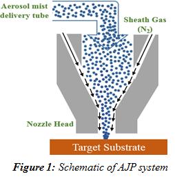
Aerosol jet works on atomization of materials for establishing a fine mist of microdroplets by either of the following two techniques;
- Ultrasonication
- Pressurized gases
Aerosol mist is entrained in the atomizer gas directed towards the print-head nozzle (shown in Figure 1). The annular flow of atomizer gas accompanied by sheath gas applied at the nozzle converge and densify the aerosol mist in the center of printhead. The aerodynamic gas flows guarantee the uniform high resolution patterning as well as potentially avoiding the nozzle clogging.
Aerosol jet printing enables to deposit a large variety of materials including metals, conductors, insulators, carbon based nanomaterials (CNTs, graphene…), polymers, adhesives, and biological materials for a wide range applications.
We are pushing the application of the technology on three main types of developments using the unique features of the Aerosol Jet process:
High resolution printing
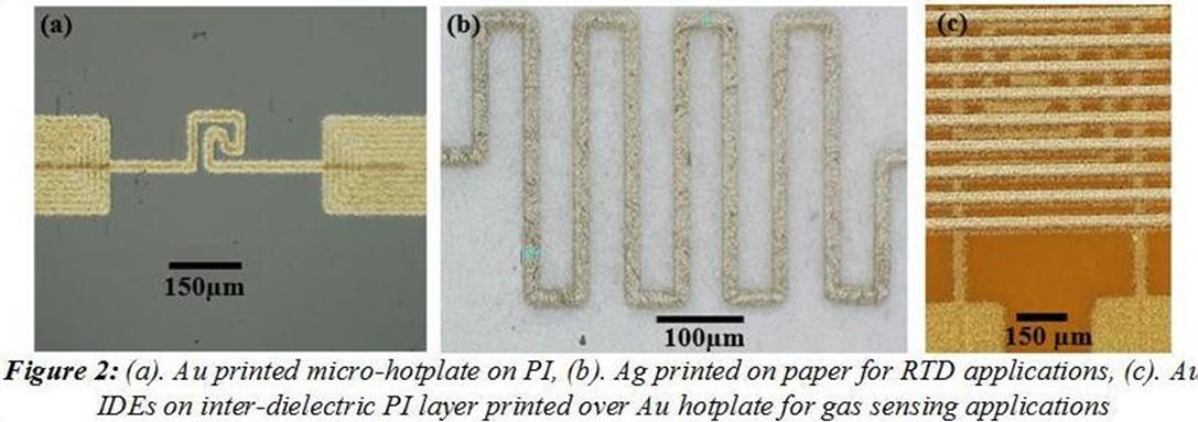
Organic materials (i.e. PEDOT-PSS, Polyimide), inorganic conductors (i.e. Au and Ag), metal-oxides semiconductor and dielectric materials, and nanostructures are printed at high resolution or on large area forming thin layers.
Hybrid printing (2.5D) on 3D-printed parts with topography
Aerosol jet is a process that can lead to conformability of the printing patterns. We are applying the technique to integrate functional components on substrates with topography or directly onto products.
Printing of multi-layer stacks and dielectric/polymeric layers
The technique is used to deposit inter-dielectric and passivation layers locally or on large area. Notably we have developed a process to print Polyimide (PI) precursor solution as an insulation layer. We are also investigating sol-gel ceramics printing for fabrication of metal-oxide thin film transistors on polymeric substrates.
References
S. Khan, D. Briand, All printed low-power metal oxide gas sensors on polymeric substrates, Flexible and Printed Electronics, 4 (2019) 015002.
S. Khan, T.P. Nguyen, M. Lubej, L. Thiery, P. Vairac, D. Briand, “Low-power printed microhotplates through aerosol jetting of gold on thin polyimide membranes” Microelectronic Engineering, 194 (2018) 71-78.